skylogger said:
Huh. So something is boosting the 13 V input, or else there are some spiky signals confusing the multimeter. But across large capacitors, this should not be the case. It seems such a non-standard value. And so unnecessary given that there is another power supply chopping it up on the next board. It's possible that it's meant to be some other value, say 20.0 V, and some fault is loading it down, but for now I think we assume it's meant to be "about 17 V" until proven otherwise.
... checked to see if there is any AC at the primaries of the transformer that are on the ouptus of the IGBT's. This is still dead.
This is to be expected, considering we still have about three other balls to juggle.
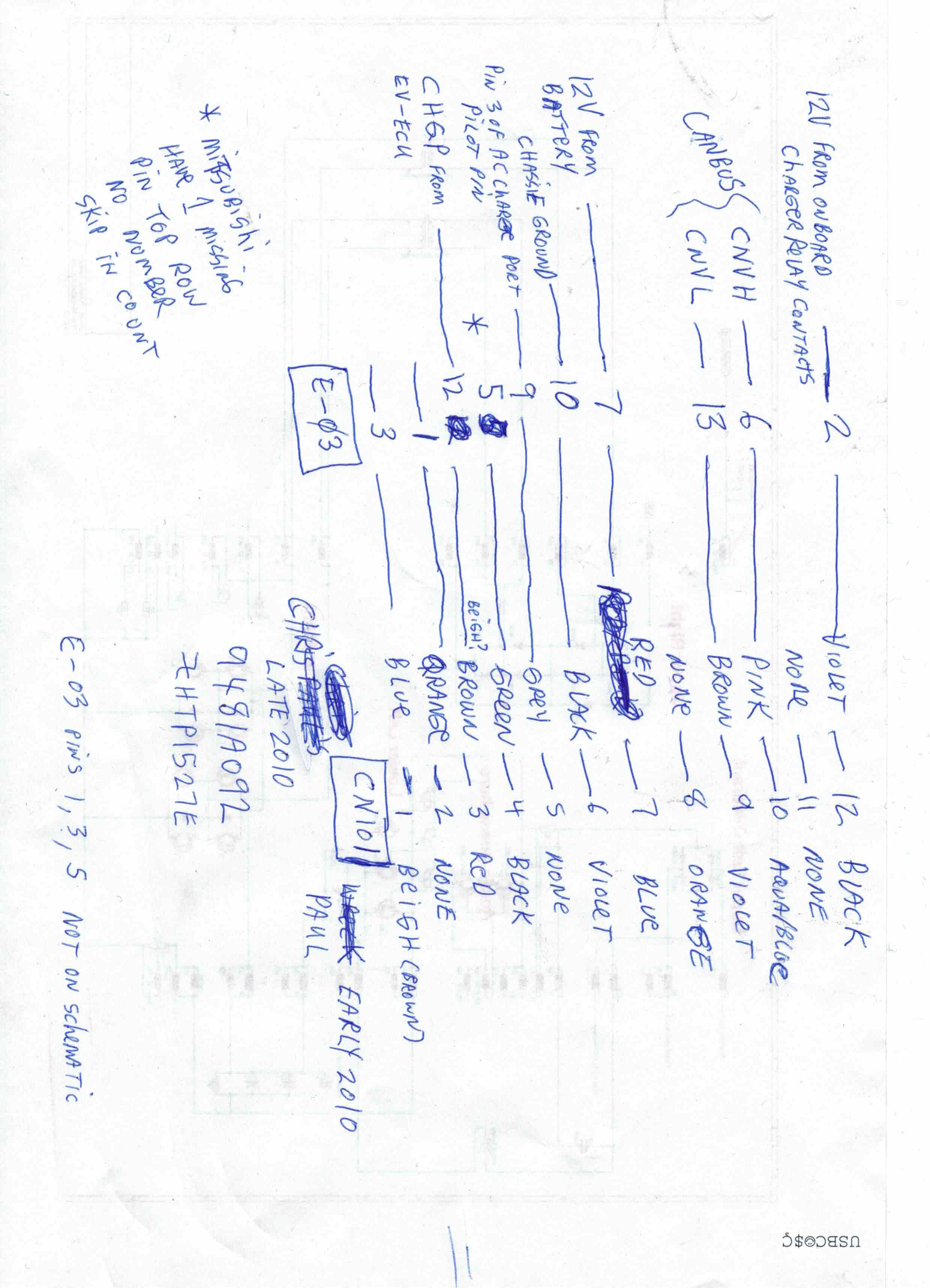
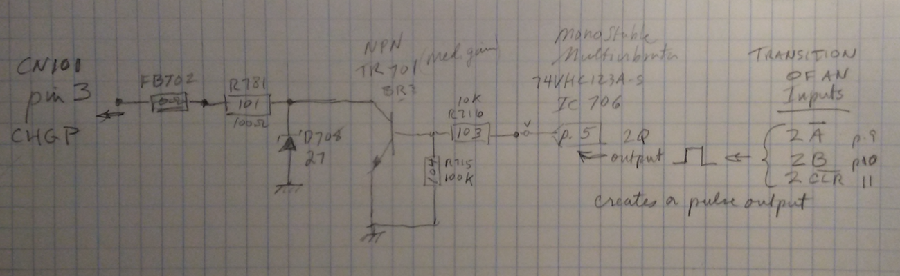
We probably need to work out what signal needs to be on the CHGP Line from the EV-ECU to pin 3 of CN101. This is probably the signal that actually enables/disables the running of the IGBT's.
Yes, this is the first one. I note that the proximity signal from the J1772 connector (that Mitsubishi are calling pin 4, but the rest of the world calls pin 5) goes straight to the EV-ECU. So when the user presses the button (meaning stop charging, I believe, but I'm no J1772 expert as yet), this must go via the EV-ECU and the only ways to stop the charge are via the CHGP signal, or by cutting the power to the charger relay. The latter seems way too crude to me; you want to gracefully shut down the power, after immediately cutting off gate drive to the main IGBTs to stop charging. Otherwise, you could have IGBTs with partial gate drive going into linear regions and overheating.
I'm also having problems working out the The PE and CP Proximity and Pilot pins from the j1772 connector to the charger for bench testing.
I think that PIN 4 of the J1772 is an output to EVSE to tell it what charge status is on car based on change in resistor values. This was not fully implemented on 2010 I-MIEV, and since it's an output, it not required to get charger enabled for bench testing.
My understanding is that proximity is a signal to the vehicle, so it can tell one of three states: no plug connected, connected but button not pressed, and connected with button pressed. You might measure the voltage to chassis at the proximity pin; not connected should be 4.5 V due to a 330 Ω pullup to 5.0 V and the 2.74 kΩ pulldown near the J1772 socket. If so, try putting a 150 Ω resistor to chassis so that the pin falls to 1.5 V. You might consider putting a switch in series with that resistor, perhaps a normally closed one, with a 330 Ω resistor across that switch. Then if something goes wrong, you press that switch in a hurry, and it's like pressing the J1772 plug button, which I believe should kill the charging. Maybe even make it a red mushroom type (an E-stop for charging).
Pin 5 on the J1772 is the proxiity pin that confirms the charger cable is plugged in. I think this pin connects to ground when a charger cable is attached.
Again, my understanding is that when the cable is attached, that pin 5 (according to the rest of the world, or pin 4 on the Mitsubishi diagram) needs 150 Ω to ground to indicate cable presence. A short circuit to ground would be 0 V, an error, and would likely prevent charging.
Pin 5 on the Mitsubishi diagram is the large earth pin at the bottom, which the rest of the world calls pin 3. Some diagrams show it as neutral in split phase situations, but fortunately you don't have that. All the diagrams I see show the vehicle connecting it to chassis / earth / ground. This seems to be the reference for the pilot and proximity signals.
I note that the pilot signal is generated by the EVSE, and "read" by the charger, although the charger modifies its amplitude with a diode and two different valued resistors. It might be necessary to generate a ±12 V 1 kHz square wave (24 V p-p) with a 1K resistor in series to keep the EV-ECU happy. It might be necessary to start with DC +12 V to initiate the handshaking (state A, EVSE ready, not connected).
If this is true, then this would connect to pin 9 of connector E-01 which in turn connects to pin 5 of the CN101 Connector on the TOP PCB. It looks like this pin is not connected on the early 2010 model, but is connected in the late 2010 model.
I'm confused. Pin 9 of E-01 connects to pin 3 of the J1772 socket per the Mitsubishi diagram. This seems to be the pilot signal, that the rest of the world calls pin 4. It makes sense if these are not connected in early 2010 models, since they don't do real J1772 charging, and merely connect the mains (large pins 1, 2) to a mains plug (forgive me if I got this wrong). I thought all Australian 2010 models are like this, unless or until they have the "Gelco" modification, which makes them more or less proper J1772 compliant, so you can charge at public charging stations. @Skylogger, has your 2010 had the "Gelco" modification done? Does yours connect to the pilot signal (rest of the world pin 4, Mitsubishi pin 3)?
I note that the confusion re pin numbering is merely the number that's the problem; the function (e.g. line / pilot / proximity / protective earth) is the same, as it needs to be to work with public charging stations.
I think this would mean that Pin 5 of CN101 would need to be connected to ground before the charger would run.
Kiev / Coulomb: do you have any info on this to confirm this?
As above, I disagree, but am happy to be proved wrong.
[ Edit: "no button" -> "button not pressed" ]